 Inorganic process facilities:
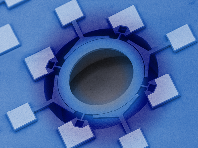
- Lithography - ultimate resolution optical, nanoimprint and electron beam lithography
- Etching processes - wet etching, RIE and focussed ion beam milling (including dual beam FIB’s)
- Deposition - thermal and e-beam evaporators, DC and RF magnetron sputter systems, high temperature MOCVD, MBE, PECVD.
Organic processing facilities:
- Wet chemistry laboratories
- CVD systems and furnaces for nanotubes and nanowire growth
- Ink-jet printing facilities for organic electronics
Whether you are looking for novel organic or inorganic materials, require world-leading expertise in e-beam or photolithography, or need nanotube or nanowire morphologies, or prefer to develop devices using self-assembly, we can find the right experts to address your needs. The University has expertise in the fabrication of:
- Semiconductor devices – Si, SOI, SiGe, GaAs, AlGaAs, InP, GaN and diamond
- Thin Films – optical coatings, piezoelectric films, diamond-like-carbon, ferromagnetic and other materials can be produced using sputtering, CVD, thermal or e-beam evaporation, laser ablation, spray coating and sol gel processes.
- Nano-materials – carbon nanotubes (CNT’s), nanoflowers, graphene, ZnO, SiC, TiO2 and VO nanowires, quantum dots, sol gels, colloids and precursors
- Polymers and polymer films – conducting, liquid crystal, light emitting, light absorbing and inert polymers formed either through self assembly, ink-jet printing or soft nano-imprint lithography (NIL).
Once we have fabricated your devices, we can test them using a vast range of characterisation techniques to evaluate performance. Please see our characterisation section to find which techniques are available and may be suited to your needs.
| If you would like more information on any equipment, usage costs or access please contact us. |