Scanning Electron Microscopy (SEM)
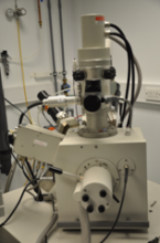
The Cambridge Nanoscience Centre houses a LEO GEMINI 1530VP FEG-SEM system, a scanning electron microscope which uses a very fine electron beam for imaging micro and nanoscale objects. It can be used in imaging as well as EDX mode for local elemental analysis. It has inlens, secondary electron and quadrant back scatter detectors. It has a field emission electron source. Electron beam energy can be varied from 200V to 30KeV. It can also be operated at variable pressure.
Focussed Ion Beam Milling (FIB)
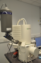
The Cambridge Nanoscience Centre offers an FEI 200 focussed ion beam milling system for device failure analysis, circuits modification and prototyping micro and nano devices. The Ga FIB system is very similar to the SEM but it uses Ga ions rather than electrons. Ga ions physically mill the material locally when they strike the surface. This property is used for fabricating nano and microstructures. As well as milling, the Ga FIB can also deposit materials. When a metal precursor gas is injected into the system, Ga ions nail down the metal to the surface and the volatile compounds are pumped away. Pt and SiO2 can be deposited in our FIB system.
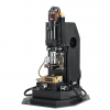
FEI Titan Krios Transmission Electron Microscope (TEM)
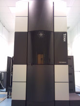
The Titan is the first and only S/TEM designed to fully realize the benefits of corrected S/TEM. Aberration correction breaks through the fundamental optical limitations of magnetic lenses, but requires equally fundamental changes in system design to achieve the stability required for ultra high resolution imaging and analysis. The Titan's extra wide column was specifically designed to give the mechanical stability required due to the added height of probe and image correctors. Its proprietary constant power lenses and advanced power supplies provide the necessary thermal and electronic stability.
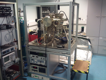
Scanning Tunneling Microscopy (STM)
Vestibulum bibendum eros sit amet lectus ullamcorper sit amet placerat arcu euismod. Vestibulum a nisi non lectus ornare pulvinar. Duis consectetur, tellus ultrices tincidunt pulvinar, arcu mauris vulputate arcu, in porta ipsum mauris vitae libero. Curabitur ac scelerisque odio. Fusce a semper justo. Integer vel velit vitae tortor dapibus pretium et eget urna. Integer lorem nisl, fermentum semper elementum vitae, mollis id eros. Etiam pharetra, enim a sollicitudin condimentum, elit risus dignissim odio, eu rhoncus nisi lorem vel mauris. Donec et tellus tortor, sed molestie ligula. Suspendisse lacus tortor, tempus id iaculis eu, vestibulum non ipsum. Maecenas ac augue risus, dapibus ultrices tellus. Ut id lectus in elit auctor dictum.
The XE-100 low drift automated step and scan AFM is the perfect tool for non-contact use in materials science, polymers, electrochemistry and other applications in nanoscience and engineering.