CRESTEC CABL 9000C E-Beam Lithography System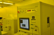 The Cambridge Nanoscience Centre offers access to a high-resolution electron beam lithography system, the CABL 9000C from CRESTEC Corporation Ltd Japan. CRESTEC is the world leader in high-resolution e-beam lithography tools. It is the first system to be installed in the UK. The CABL 9000C is a highly sophisticated electron beam lithography system with a beam diameter of 2nm and line stitching accuracy of 20nm
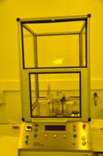 Obducat Eitre Nano-Imprint Lithography Individually or in combination with e-beam lithography, the Obducat Eitre NIL system can be used for large-area device nanofabrication. Nano Imprint Lithography (NIL) is an emerging lithographic technology that promises high throughput patterning of nanostructures. With NIL it’s possible to achieve sub-10nm resolution features over large areas. NIL can significantly simplify the production of nanostructures using a wide variety of materials. NIL intrinsically has better dimensional control that can be achieved using conventional UV lithography.
Karl Suss MJB4 Mask Aligner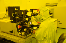 Easy to use and compact in size the SUSS MJB4 represents the perfect system for laboratories and small volume production. As an inexpensive photolithography solution the MJB4 has set industry standards specifically for processing of small substrates and pieces up to 100 mm. Equipped with a reliable, high precision mask alignment and high resolution printing capability in the submicron range the MJB4 demonstrates a performance unsurpassed by any comparable machine.
Karl Suss MJB3 Mask Aligner The Karl Suss MJB3 Contact Aligner system can perform precision mask-to-wafer (sample) 1:1 contact printing in hard contact mode. It can accommodate exposure of irregularly shaped substrates and standard wafers up to 3”.
Wafer preparation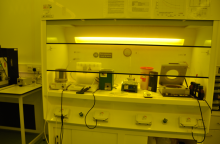 POLOS Spin Coaters suitable for single wafer Cleaning, Rinse/Dry, Coating, Developing & Etching specifically designed for MEMS & Semiconductors.