We have an extensive range of characterisation and analysis facilities for analysing micro and nano devices, semiconductors, nano-materials, electronic circuits, thin films, elastomers and polymers.
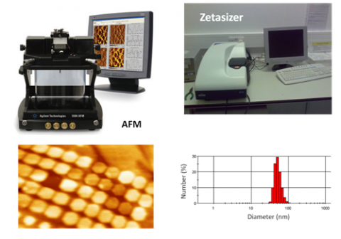
We have particular experience in nanoscale materials. Our characterisation facilities include optical microscopy; scanning electron microscopy; atomic force microscopy; magnetic force microscopy; scanning tunnelling microscopy; dynamic optical sizing; focused ion beam; surface profilometry and multi-probe stations for nanoscale electrical testing.
 |
|
 |
|
|
||

If you don’t know which technique is best for the job in hand, or can’t see the characterisation equipment you need listed above, please contact us and we can advise you either on alternative techniques or put you in touch with other centres with complementary facilities.