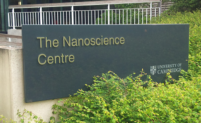
Note: Add @cam.ac.uk to the ends of email addresses. The reason they are not already added is an attempt to stop spam mail.
Dielectrophoresis
|
 |
| Dielectrophoresis |
|
| Project Staff: Will Winter, Mark E Welland |
| Email: Send Email |
|
 |
| This project investigates the use of dielectrophoresis to measure the dielectric properties of particles in a fluid channel. Numerical modeling of dielectrophoretic effects (including particle to particle interactions) is performed to aid in the design of electrodes and translate particle behavior into dielectric properties. |
| More Information... |
 |
|
Aggregation of proteins and peptides
|

AFM image of amyloid fibril |
| |
|
| Project Staff: Tuomas Knowles, Mark E Welland |
| Email: Send Email |
|
 |
| It is becoming clear that the amyloid fold is naturally exploited under carefully controlled conditions for example for functional bacterial coatings, giving rise to the idea that fibrillous protein structures could find use in material science applications. Our research is centered around developing a quantitative understanding of the processes involved in the transition from the native soluble form of proteins into polymeric fibrils. |
| More Information... |
 |
|
Novel Method for the Electrical Characterization of DNA
|
 |
| Carbon Nanotube on an AFM Tip |
|
| Project Staff: Paul B. Rhatigan, Mark E Welland |
| Email: Send Email |
|
 |
| The inclusion of biological molecules into nanoscale electrical devices has many potential applications in biomedical engineering, biosensors, and molecular electronics. This project aims to utilize nanofabrication techniques to create a novel method for electrically characterizing individual nanostructures, including DNA. |
| More Information... |
 |
|
Nanometre-scale characterization of electrical properties of conducting polymers
|
 |
| Nanometre-scale charaterization of electrical properties of conducting polymers |
|
| Project Staff: Nan Wang, Mark E Welland |
| Email: Send Email |
|
 |
| This project is aiming to characterize some specific conducting polymers using Scanning Probe Microscopy (SPM). The polymer has an intrinsic stiff-rod structure with a conductive centre surrounded by an insulating shell structure, realizing an ideal molecular wire. SPM is used to explore not only their detailed structures but also their physical properties such as electrical properties on the nm scale. |
| More Information... |
 |
|
Chemical Specification at the Nanoscale by Scanning Probe Microscopy
|
 |
| Friction force image taken using lateral force microscopy |
|
| Project Staff: Simon Attwood, Mark E Welland |
| Email: Send Email |
|
 |
| The Overall aim of the project is to develop techniques for chemical analysis of nanostructures based on scanning probe methods. There is a requirement for quantitative methods to determine the chemical state of nanostructures both from a research prospective but also as a metrology tool for developing standards. |
| More Information... |
 |
|
Spin@RT
|
 |
| CPP nano-pillars fabricated using 3D Ga-FIB milling |
|
|
Production of Structural Colour Coatings via Patterning of Hybrid Multilayer Films
|
 |
| Structural colour coating sample |
|
| Project Staff: Mathias Kolle, Ulli Steiner |
| Email: Send Email |
|
 |
| The first step of this project is the development of hybrid organic-inorganic multilayer structures with adequate optical properties using a high refractive inorganic material such as PbS, TiO2 or ZrO2 and a low refractive index polymer. Subsequently a procedure to pattern the obtained multilayer films shall be developed by taking advantage of special electro-hydrodynamic pattern formation techniques. These techniques are already well established in the "Thin Films and Interfaces" group of Prof. Steiner for the patterning of single liquid films. |
| More Information... |
 |
|
Light emission from Inorganic Nanostructures - the STABILIGHT project
|
 |
| Light emitting nanoparticles |
|
| Project Staff: James S Bendall, Mark E Welland |
| Email: Send Email |
|
 |
| The aim of STABILIGHT is the design and demonstration of novel nano-photonic devices based on all inorganic nanostructured materials operating at low DC voltage with enhanced photoemission activity and thermal stability to be used both in passive and active (transistor) light emitting devices. Materials and technologies involved are addressed to large consumer-markets such as automotive, information displays and lighting. |
| More Information... |
 |
|
Advanced Electron Microscopy Investigations Of Nanoparticle-Cell Interactions
|

Uptake of C60 into human macrophage cells |
| |
|
| Project Staff: Crystal Cheng, Mark E Welland |
| Email: Send Email |
|
 |
| The objective of this project has been to develop novel methodologies to image carbon-based nanoparticles within cellular compartments using state-of the-art TEM techniques. We have been able to use both high angular annular dark field (HAADF) STEM imaging and energy-filtered TEM (EFTEM) in tomographic studies to evaluate the distribution of C60 nanoparticles, within the cell. |
| More Information... |
 |
|
Oxide nanostructures for CMOS Integration
|
|
SEM and TEM images of Single Crystalline VO2 nanowires |
| Project Staff: Jung Inn Sohn, Heungjin Joo, Mark E Welland |
| Email: Send Email |
|
 |
| The aim of this project is to explore the technological potential of oxide nano-materials with both in terms of their physical properties but also with a view of potential fabrication routes for future devices. The research interests cover challenging issues in the following areas:
1. Controlled growth and assembly of oxide nanowires
2. Characterization of oxide nanowires and design of device
3. System integration
|
| More Information... |
 |
|
Functional Nanostructures
|
 |
| ZnO nanowire array |
|
| Project Staff: Lukas Schmidt-Mende, Natalie Plank, Mark E Welland |
| Email: Send Email |
|
 |
| Functional Nanostructures for Hybrid Solar Cells One current project aims to fabricate hybrid solar cells combining metal-oxide nanostructures and organic materials. The control of film morphology, alignment of molecules and controlled assembly of materials at the nanometer scale is necessary for efficient devices. This research will address the control of the structure of the active layer by introducing a nano-structured metal-oxide electrode as a template for the organic materials. |
| More Information... |
 |
|
Scanning Probe Microscopy
|

Atomic resolution STM image of HOPG |
| |
|
| Project Staff: Colm Durkan, Farouk Hadeed , Yachin Ivry |
| Email: Send Email |
|
 |
| We carry out research in the general area of Nanotechnology. More specifically, we work in Scanning Probe Microscopy (SPM), in electronic transport physics, and related topics. Research interests lie in the understanding of the magnetic and electronic properties of materials and structures at the nanometer scale. |
| More Information... |
 |
|
|